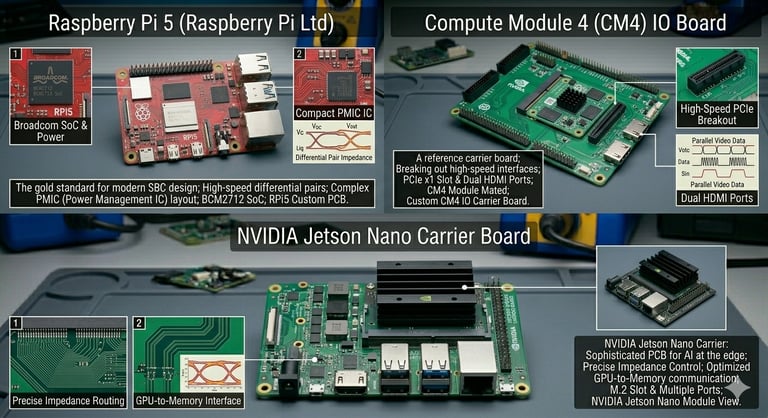
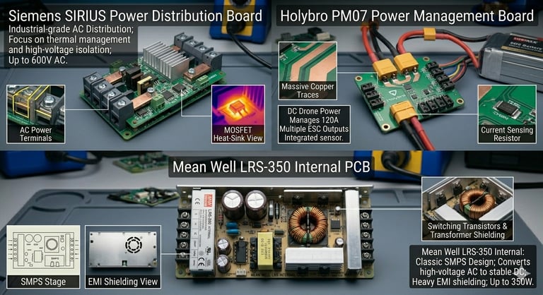
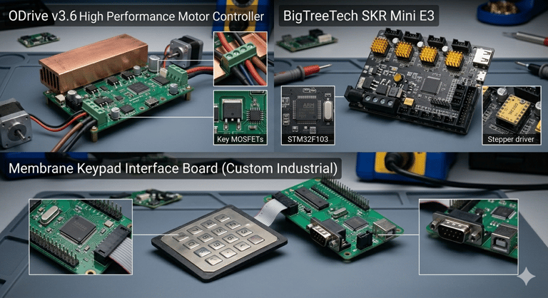
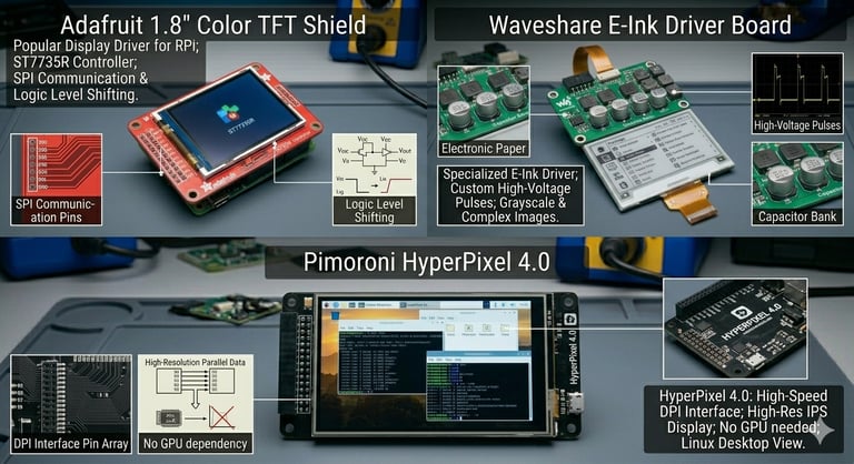
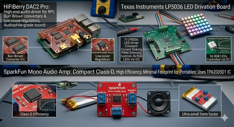
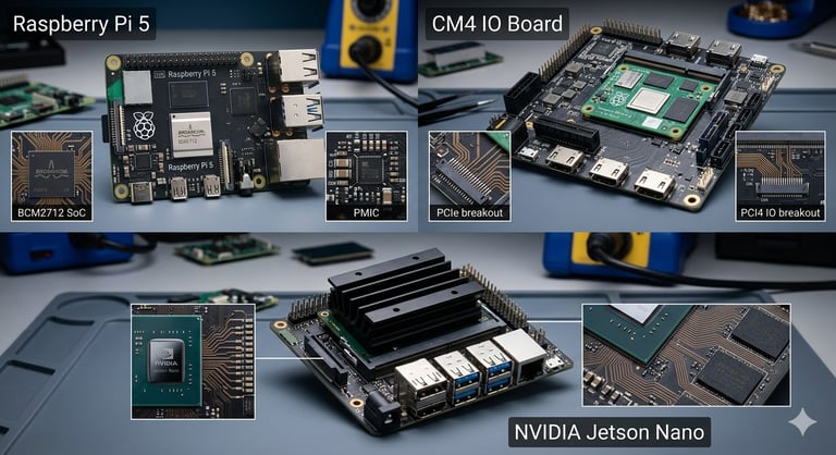
Our Projects
High-profile PCB projects and boards from leading tech companies, spanning industrial power, audio, and high-performance computing.
Our Technical Core
Advanced Engineering for High-Performance Hardware.
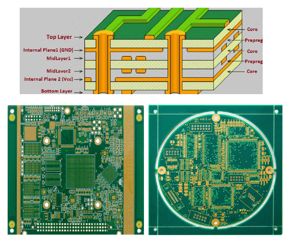
PCB Engineering & Signal Integrity
We specialize in High-Density Interconnect (HDI) and High-Speed Digital Design. Our engineering process accounts for the electrical behavior of traces at high frequencies to ensure rock-solid reliability.
Controlled Impedance Routing: Precision matching for 50Ω/100Ω differential pairs (USB 3.0, HDMI, Ethernet).
Layer Stack-up Optimization: Custom dielectric selection (FR-4, Rogers) to minimize Crosstalk and Reflections.
Advanced Vias: Expertise in Blind and Buried Vias for space-constrained IoT and wearable designs.
Mixed-Signal Isolation: Strict split-plane management to prevent digital noise from bleeding into sensitive analog circuits.
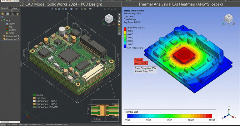
Simulation-Driven Development
We use industry-standard simulation tools to "fail fast" in the virtual world, saving you thousands in physical spin costs.
Pre-Compliance EMI/EMC Analysis: Identifying radiation bottlenecks before you hit the test lab (FCC/CE/CISPR standards).
SI/PI Analysis: Eye Diagram and IBIS Model simulations to verify signal timing and power rail stability (DC IR-Drop).
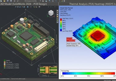
Thermal Management: Predictive heat-map modeling for active/passive cooling and heat-sink integration.
Reverse Engineering: Precision reconstruction of legacy hardware including high-accuracy analog signal path analysis.

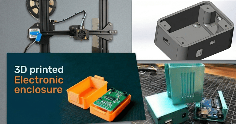
Rapid Prototyping & Enclosure Design
We bridge the gap between electronics and mechanics through Functional Prototyping.
Precision 3D Modeling: Full CAD integration for Form, Fit, and Function (FFF) validation.
FDM Prototyping: High-resolution in-house printing with engineering-grade materials (PLA, ABS, PETG).
Custom Test Rigs: Design and assembly of dedicated Functional Test Fixtures for production-line verification.
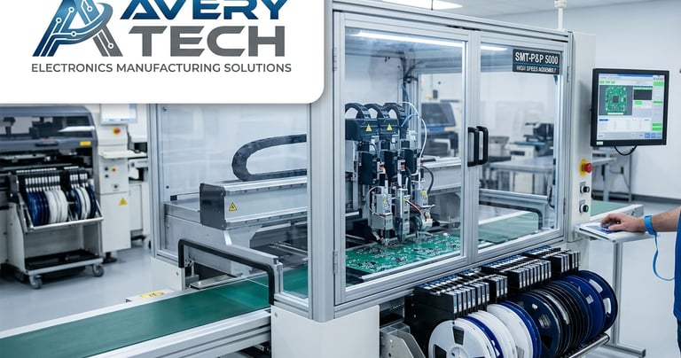
The Path to Production (DFM/DFA)
A design is only as good as the factory’s ability to build it. We offer End-to-End Design-to-Manufacturing Support.
Design for Manufacture (DFM): Rigorous review of copper clearance, annular rings, and solder mask expansion to maximize yield.
Design for Assembly (DFA): Optimizing component placement for automated Pick-and-Place and reflow profiles.
Turnkey Manufacturing: Direct liaison with Avery Tech (Bangalore) for seamless Gerber/ODB++ hand-offs and PCBA oversight.